| CPC H01L 29/66795 (2013.01) [H01L 21/02236 (2013.01); H01L 21/02532 (2013.01); H01L 21/823418 (2013.01); H01L 21/823431 (2013.01); H01L 21/823468 (2013.01); H01L 27/0886 (2013.01); H01L 29/0673 (2013.01); H01L 29/0847 (2013.01); H01L 29/42392 (2013.01); H01L 29/6653 (2013.01); H01L 29/66545 (2013.01); H01L 29/66553 (2013.01); H01L 29/66636 (2013.01); H01L 29/7851 (2013.01); H01L 29/78696 (2013.01); H01L 29/0653 (2013.01); H01L 29/6656 (2013.01)] | 20 Claims |
|
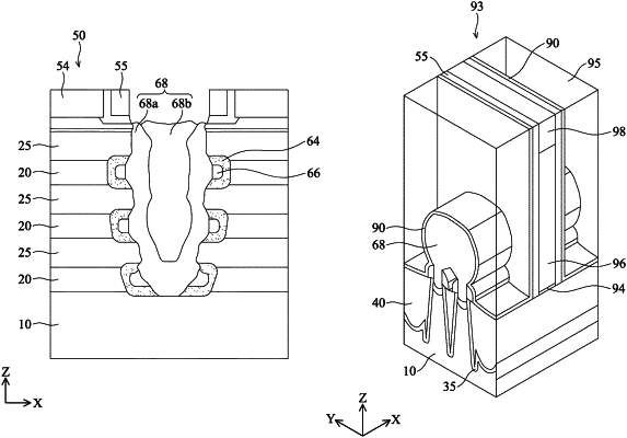
1. A semiconductor device, comprising:
channel members vertically stacked over a substrate;
a gate structure engaging the channel members;
a gate spacer layer disposed on sidewalls of the gate structure;
an epitaxial feature abutting the channel members;
an inner spacer layer interposing the gate structure and the epitaxial feature; and
a semiconductor layer interposing the inner spacer layer and the epitaxial feature.
|
|
11. A semiconductor device, comprising:
one or more channel layers over a substrate;
a gate structure engaging the one or more channel layers;
a source/drain (S/D) formation assistance region partially embedded in the substrate, wherein the S/D formation assistance region includes a semiconductor seed layer embedded in an isolation layer, and wherein the isolation layer electrically isolates the semiconductor seed layer from the substrate; and
an S/D epitaxial feature connecting to the semiconductor seed layer and the one or more channel layers.
|
|
18. A semiconductor device, comprising:
channel members vertically stacked over a substrate;
a gate structure wrapping around each of the channel members;
an epitaxial feature abutting the channel members;
an isolation layer in physical contact with the epitaxial feature and the gate structure; and
a semiconductor layer in physical contact with the epitaxial feature and the isolation layer, wherein a top surface and a bottom surface of the semiconductor layer is covered by the isolation layer.
|