| CPC H01L 29/516 (2013.01) [H01L 29/42364 (2013.01); H01L 29/42392 (2013.01); H01L 29/4966 (2013.01); H01L 29/78696 (2013.01)] | 19 Claims |
|
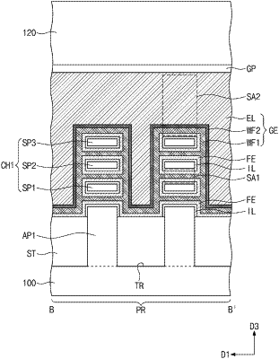
1. A semiconductor device comprising:
a substrate including an active pattern;
a device isolation layer on the substrate and in a trench that defines the active pattern;
a plurality of semiconductor patterns that are stacked on the active pattern and are spaced apart from each other in a vertical direction;
a plurality of ferroelectric patterns on the plurality of semiconductor patterns, respectively; and
a gate electrode on the plurality of ferroelectric patterns,
wherein, in a cross-sectional view taken along a longitudinal direction of the gate electrode:
the plurality of ferroelectric patterns are spaced apart from each other in the vertical direction,
each of the plurality of ferroelectric patterns is between the gate electrode and a respective one of the plurality of semiconductor patterns,
each of the plurality of ferroelectric patterns surrounds a respective one of the plurality of semiconductor patterns,
the gate electrode includes a work function metal pattern and an electrode pattern,
the work function metal pattern is in a space between adjacent ones of the plurality of ferroelectric patterns, and
the space between the adjacent ones of the plurality of ferroelectric patterns is free of the electrode pattern.
|