| CPC H01L 29/41791 (2013.01) [H01L 21/823462 (2013.01); H01L 21/823857 (2013.01); H01L 27/0886 (2013.01); H01L 29/0673 (2013.01); H01L 29/42364 (2013.01); H01L 29/42392 (2013.01); H01L 29/513 (2013.01); H01L 29/66439 (2013.01); H01L 29/775 (2013.01); H01L 29/785 (2013.01); H01L 29/78696 (2013.01)] | 20 Claims |
|
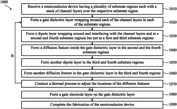
1. A method, comprising:
forming a dielectric layer on a semiconductor workpiece;
forming a first patterned layer of a first dipole material on the dielectric layer;
performing a first thermal drive-in operation at a first temperature to form a diffusion feature in a first portion of the dielectric layer beneath the first patterned layer;
forming a second patterned layer of a second dipole material, a first section of the second patterned layer being on the diffusion feature and a second section of the second patterned layer being offset from the diffusion feature;
performing a second thermal drive-in operation at a second temperature, wherein the second temperature is less than the first temperature; and
forming a gate electrode layer on the dielectric layer.
|