| CPC H01L 29/41775 (2013.01) [H01L 27/0924 (2013.01); H01L 29/0665 (2013.01); H01L 29/41733 (2013.01); H01L 29/41791 (2013.01); H01L 29/42392 (2013.01); H01L 29/7851 (2013.01); H01L 29/786 (2013.01)] | 20 Claims |
|
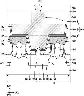
1. A semiconductor device comprising:
a substrate including a first region and a second region, the second region being adjacent to the first region in a first horizontal direction;
a first active pattern extending in a second horizontal direction on the first region, the second horizontal direction being different from the first horizontal direction;
a second active pattern extending in the second horizontal direction on the second region, the second active pattern being spaced apart from the first active pattern in the first horizontal direction;
a field insulating layer surrounding at least a part of side walls of each of the first and second active patterns on the substrate, the field insulating layer including a protrusion protruding upwardly in a vertical direction on a boundary line between the first region and the second region;
a gate electrode extending in the first horizontal direction on the first and second active patterns;
a first source/drain region on at least one side of the gate electrode on the first active pattern;
a second source/drain region on at least one side of the gate electrode on the second active pattern; and
a source/drain contact electrically connecting the first source/drain region and the second source/drain region with each other, the source/drain contact including a first portion and a second portion, the first portion extending toward the field insulating layer between the first source/drain region and the second source/drain region, the second portion on the first portion,
wherein a lower surface of the first portion of the source/drain contact includes a recess which is recessed upwardly in the vertical direction, and
at least a part of the protrusion is inside the recess.
|