| CPC H01L 29/41766 (2013.01) [H01L 29/1029 (2013.01); H01L 29/2003 (2013.01); H01L 29/41725 (2013.01); H01L 29/66462 (2013.01); H01L 29/7786 (2013.01); H01L 29/7838 (2013.01)] | 9 Claims |
|
1. A semiconductor device, comprising:
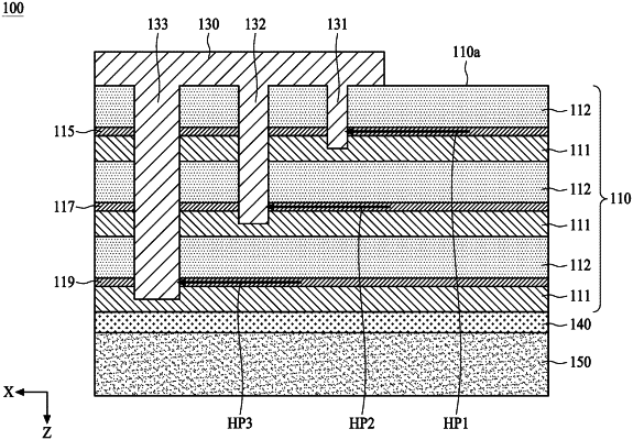
a semiconductor heterostructure layer, comprising alternating first semiconductor material layers and second semiconductor material layers, wherein a two-dimensional hole gas (2DHG) is generated between each first semiconductor material layer and its above adjacent second semiconductor material layer; and
a conductive structure, comprising a plurality of conductive fingers extending from a surface of the semiconductor heterostructure layer into the semiconductor heterostructure layer, wherein the plurality of conductive fingers are arranged in a first direction substantially parallel to the surface, and wherein lengths of the plurality of conductive fingers progressively increase in the first direction so that an end portion of each conductive finger is respectively positioned in a different first semiconductor material layer and is in contact with the 2DHG, and widths of the plurality of conductive fingers gradually increase in the first direction.
|