| CPC H01L 29/41741 (2013.01) [H01L 21/823871 (2013.01); H01L 21/823885 (2013.01); H01L 27/092 (2013.01); H01L 27/0924 (2013.01); H01L 29/0653 (2013.01); H01L 29/42376 (2013.01); H01L 29/7827 (2013.01); H01L 29/785 (2013.01)] | 14 Claims |
|
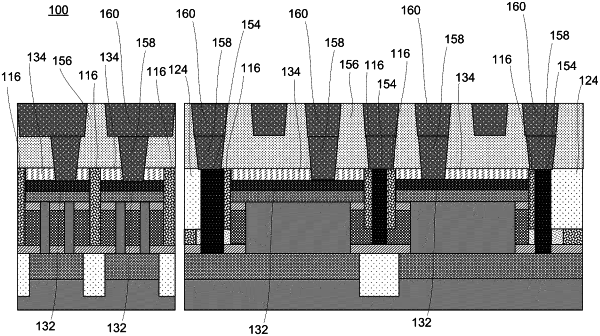
1. A semiconductor device comprising:
a channel fin between a bottom source/drain (S/D) region and a top S/D region;
a gate around the channel fin, the gate comprising a first gate portion directly connected to a first side of the channel fin and a second gate portion directly connected to a second side of the channel fin, the first gate portion comprising a first sidewall and a second sidewall, and the second gate portion comprising a third sidewall;
a top metallization upon the top S/D region;
a first contact metallization connected to the first sidewall of the gate;
a second contact metallization connected to the bottom S/D region;
a vertical liner comprising a first vertical liner portion directly connected to at least the second sidewall of the gate and directly connected to a sidewall of the first contact metallization and a second vertical liner portion directly connected to at least the third sidewall of the gate and directly connected to a sidewall of the second contact metallization; and
a top spacer between the gate and the top S/D region and in direct contact with the channel fin, the top spacer comprising a first sidewall that is in direct contact with the first vertical liner portion and a second sidewall that is in direct contact with the second vertical liner portion.
|