| CPC H01L 29/41733 (2013.01) [H01L 21/02236 (2013.01); H01L 21/02603 (2013.01); H01L 23/5286 (2013.01); H01L 29/0673 (2013.01); H01L 29/42392 (2013.01); H01L 29/66545 (2013.01); H01L 29/66553 (2013.01); H01L 29/66636 (2013.01); H01L 29/66742 (2013.01); H01L 29/7848 (2013.01); H01L 29/78618 (2013.01); H01L 29/78696 (2013.01)] | 20 Claims |
|
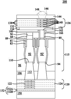
1. A device comprising:
a device layer comprising a first transistor;
a first interconnect structure on a front-side of the device layer; and
a second interconnect structure on a backside of the device layer, the second interconnect structure comprising:
a first dielectric layer on the backside of the device layer, wherein a semiconductor material is disposed between the first dielectric layer and a gate stack of the first transistor; and
a source/drain contact extending through the first dielectric layer to a source/drain region of the first transistor, wherein the source/drain contact electrically connects the source/drain region to a power rail in the second interconnect structure.
|