| CPC H01L 29/0619 (2013.01) [H01L 29/66712 (2013.01); H01L 29/7811 (2013.01); H01L 29/7813 (2013.01)] | 32 Claims |
|
1. A power semiconductor device, comprising:
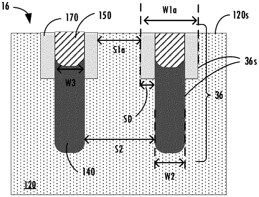
a semiconductor layer structure comprising a semiconductor drift region of a first conductivity type and an edge termination region comprising a plurality of guard rings of a second conductivity type,
wherein one or more of the guard rings extend in the semiconductor drift region to a depth of greater than about 1 micrometers (μm) relative to a surface of the semiconductor layer structure, and two or more of the guard rings are laterally separated from one another by a spacing of less than about 3 μm.
|