| CPC H01L 28/75 (2013.01) [H01L 28/60 (2013.01); H01L 28/87 (2013.01); H01L 28/88 (2013.01); H01L 28/90 (2013.01); H10B 12/0335 (2023.02); H10B 12/31 (2023.02)] | 20 Claims |
|
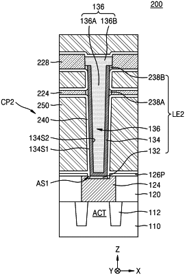
1. An integrated circuit device comprising:
a substrate;
an insulating interlayer on the substrate;
an etch stop layer on the insulating interlayer;
a lower electrode structure disposed over the insulating interlayer;
a dielectric layer disposed on the lower electrode structure; and
an upper electrode disposed on the dielectric layer,
wherein the lower electrode structure includes a first lower electrode, a second lower electrode that is disposed on the first lower electrode, and a third lower electrode that is disposed on the second lower electrode,
a bottom surface of the second lower electrode of the lower electrode structure contacts a top surface of the first lower electrode of the lower electrode structure,
the dielectric layer contacts the first lower electrode, the second lower electrode and the third lower electrode of the lower electrode structure, and
an outer bottommost point of the dielectric layer is below a topmost surface of the insulating interlayer.
|