| CPC H01L 27/156 (2013.01) [H01L 33/24 (2013.01); H01L 33/38 (2013.01); H01L 33/44 (2013.01)] | 20 Claims |
|
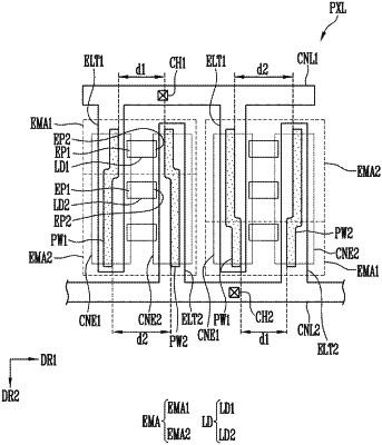
1. A light emitting device comprising:
a first emission area comprising a first light emitting diode;
a second emission area comprising a second light emitting diode;
at least one pair of first and second partition walls in each of the first emission area and the second emission area, wherein the at least one pair of first and second partition walls are facing each other;
at least one first electrode on a first partition wall of the at least one pair of first and second partition walls to cover the first partition wall, wherein the at least one first electrode is electrically connected to a first end of at least one of the first and second light emitting diodes; and
at least one second electrode on a second partition wall of the at least one pair of first and second partition walls to cover the second partition wall, wherein the at least one second electrode is electrically connected to a second end of at least one of the first and second light emitting diodes,
wherein the at least one pair of first and second partition walls have, in the first emission area, a structure different from a structure thereof in the second emission area.
|