| CPC H01L 27/14634 (2013.01) [H01L 27/1462 (2013.01); H01L 27/14623 (2013.01); H01L 27/14636 (2013.01); H01L 27/1469 (2013.01); H01L 31/153 (2013.01)] | 16 Claims |
|
1. An imaging device comprising:
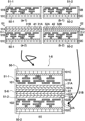
a first substrate including a first pixel array unit in which a plurality of pixels having at least a first photoelectric conversion unit that performs photoelectric conversion is arranged in a two-dimensional manner, a first wiring layer, and a first support layer stacked in this order; and
a second substrate including a second pixel array unit in which a plurality of pixels having at least a second photoelectric conversion unit that performs photoelectric conversion is arranged in a two-dimensional manner, a second wiring layer, and a second support layer stacked in this order,
wherein the first support layer and the second support layer are bonded to each other to form a stacked structure of the first substrate and the second substrate, and
at least one of the first support layer or the second support layer includes an antireflection layer.
|