| CPC H01L 27/1463 (2013.01) [H01L 27/14612 (2013.01); H01L 27/14636 (2013.01); H01L 27/14643 (2013.01); H04N 25/75 (2023.01); H04N 25/77 (2023.01)] | 14 Claims |
|
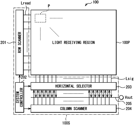
1. A solid-state imaging device, comprising:
a first semiconductor substrate comprising a plurality of unit regions and a potential adjustment region;
a photoelectric converter for each of the plurality of unit regions;
an isolation region that runs through the first semiconductor substrate in a thickness direction of the first semiconductor substrate and is configured to electrically isolate the plurality of unit regions from each other;
a charge holding section that is electrically coupled to the photoelectric converter and configured to receive signal charge from the photoelectric converter; and
a charge accumulation section that is shared by at least two unit regions of the plurality of unit regions and to which the signal charge is transferred from the photoelectric converter, wherein
the charge holding section of each of the plurality of unit regions shares the charge accumulation section, and
a potential barrier between the photoelectric converter and the charge holding section is adjusted to be smaller than a potential barrier between the photoelectric converter and the charge accumulation section based on the potential adjustment region.
|