| CPC H01L 27/14623 (2013.01) [G02B 5/207 (2013.01); G02B 5/208 (2013.01); G02B 5/26 (2013.01); G02B 5/281 (2013.01); G02B 5/288 (2013.01); H01L 27/14605 (2013.01); H01L 27/14607 (2013.01); H01L 27/14621 (2013.01); H01L 27/14627 (2013.01); H01L 27/1463 (2013.01); H01L 27/14645 (2013.01); H01L 27/14647 (2013.01); H01L 27/14649 (2013.01); H01L 27/14652 (2013.01); H01L 27/14667 (2013.01); H01L 27/14669 (2013.01); H01L 31/02165 (2013.01); H01L 31/02327 (2013.01); H01L 31/1013 (2013.01); G02B 5/265 (2013.01); H01L 2924/12043 (2013.01)] | 11 Claims |
|
1. An image sensor, comprising:
a substrate having a first region and a second region adjacent to each other; and
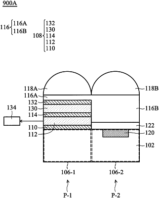
a first photoelectric conversion component disposed on the first region of the substrate, the first photoelectric conversion component being a photodiode and an infrared (IR) light detector, wherein the first photoelectric conversion component comprises:
a first metal layer formed on the substrate;
a first photoelectric conversion layer formed directly on the first metal layer;
a second metal layer formed directly on the first photoelectric conversion layer, wherein the first metal layer, the first photoelectric conversion layer and the second metal layer form a Fabry-Perot cavity that functions as the IR light detector by selectively detecting IR light by optical interference based on a wavelength of the IR light;
a first additional photoelectric conversion layer disposed directly on the second metal layer; and
a third metal layer disposed directly on the first additional photoelectric conversion layer, wherein the second metal layer, the first additional photoelectric conversion layer and the third metal layer form a first additional Fabry-Perot cavity;
a second photoelectric conversion component disposed in the second region of the substrate, wherein the second photoelectric conversion component is embedded in the substrate;
a high-k dielectric layer disposed only in the second region of the substrate;
a transparent layer disposed directly on the high-k dielectric layer and extending over the first photoelectric conversion component; and
a pad connected to the first photoelectric conversion layer,
wherein an IR light detection signal is transmitted by the first photoelectric conversion component to the pad.
|