| CPC H01L 27/14621 (2013.01) [H01L 27/14627 (2013.01); H04N 25/70 (2023.01)] | 7 Claims |
|
1. A solid-state imaging device, comprising:
a pixel array unit that includes:
a plurality of pixels one-dimensionally or two-dimensionally arrayed;
color filters;
a semiconductor substrate; and
a partition layer between the color filters, wherein
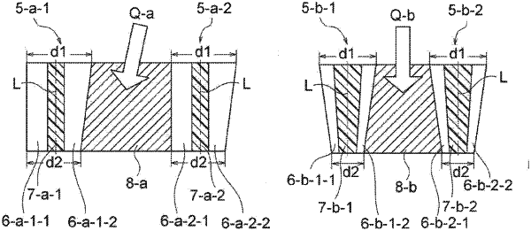
the partition layer includes a first layer on a light incident side of the pixel array unit and a second layer on a semiconductor substrate side,
the first layer has a first width on the light incident side and a third width on the semiconductor substrate side,
the second layer has a fourth width on the light incident side and a second width on the semiconductor substrate side,
the second width is different from the first width,
the first layer includes a first metal layer and a first oxide film,
the first oxide film is on the first metal layer,
the second layer includes a second metal layer and a second oxide film, and
the second oxide film is on the second metal layer.
|