US 12,009,377 B2
Solid-state imaging device and electronic apparatus for curbing deterioration of picture quality
Yutaka Ooka, Kanagawa (JP); Taizo Takachi, Kanagawa (JP); and Yuichi Yamamoto, Kanagawa (JP)
Assigned to SONY SEMICONDUCTOR SOLUTIONS CORPORATION, Kanagawa (JP)
Appl. No. 17/430,469
Filed by SONY SEMICONDUCTOR SOLUTIONS CORPORATION, Kanagawa (JP)
PCT Filed Feb. 21, 2020, PCT No. PCT/JP2020/006966
§ 371(c)(1), (2) Date Aug. 12, 2021,
PCT Pub. No. WO2020/171191, PCT Pub. Date Aug. 27, 2020.
Claims priority of application No. 2019-029911 (JP), filed on Feb. 21, 2019.
Prior Publication US 2022/0115427 A1, Apr. 14, 2022
Int. Cl. H01L 27/146 (2006.01); G02B 3/00 (2006.01); H01L 23/544 (2006.01)
CPC H01L 27/14618 (2013.01) [H01L 23/544 (2013.01); H01L 27/1462 (2013.01); H01L 27/14623 (2013.01); H01L 27/14627 (2013.01); H01L 27/14683 (2013.01); G02B 3/0056 (2013.01); H01L 2223/54426 (2013.01)] 19 Claims
OG exemplary drawing
 
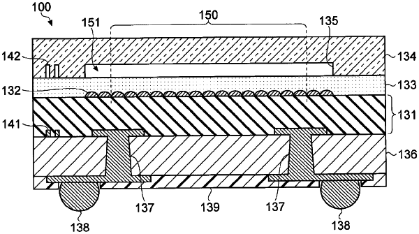
1. A solid-state imaging device, comprising:
a semiconductor substrate including a light-receiving element;
an on-chip lens disposed on a first surface of the semiconductor substrate;
a resin layer that covers the on-chip lens; and
a glass substrate disposed on a side of the first surface of the semiconductor substrate separately from the resin layer, wherein the glass substrate includes a first trench in a surface that faces the semiconductor substrate.