| CPC H01L 27/1461 (2013.01) [H01L 27/14607 (2013.01); H01L 27/14621 (2013.01); H01L 27/14627 (2013.01); H01L 27/14645 (2013.01); H04N 23/741 (2023.01)] | 15 Claims |
|
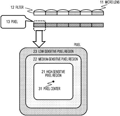
1. An imaging device, comprising:
an imaging element;
an individual micro lens for each pixel that constitutes the imaging element, wherein
each pixel of the imaging element includes:
a first sensitive pixel region at a central portion of the pixel; and
a second sensitive pixel region that surrounds the high-sensitive pixel region, and
central positions of the high-sensitive pixel region and the low-sensitive pixel region coincide with each other; and
an output control unit configured to calculate a pixel value corresponding to a pixel by a combination process of outputs of photodiodes (PDs) each being set corresponding to one of a plurality of pixel regions with different sensitivities.
|