| CPC H01L 27/14605 (2013.01) [H01L 27/14621 (2013.01); H01L 27/14627 (2013.01); H01L 27/1463 (2013.01); H01L 27/14634 (2013.01); H01L 27/14636 (2013.01); H01L 27/1464 (2013.01); H01L 27/14645 (2013.01); H04N 25/13 (2023.01); H04N 25/704 (2023.01)] | 20 Claims |
|
1. An image sensor comprising:
a substrate comprising a first surface and a second surface opposite to the first surface;
a first pixel region;
a second pixel region;
a third pixel region;
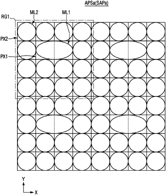
a first lens on the first pixel region;
a second lens on the second and third pixel regions;
an element separation film provided in the substrate and being interposed between the first pixel region the second pixel region;
a first color filter configured to transmit light focused by the second lens to the second pixel region and the third pixel region; and
a color filter grid forming a region in which the first color filter is provided,
wherein a width of the first pixel region in a first direction is between 0.5 um and 0.9 um,
wherein the first lens is disposed on the second surface, and
wherein the first direction is parallel to the second surface.
|