| CPC H01L 27/142 (2013.01) [H01L 27/14643 (2013.01)] | 14 Claims |
|
1. An imaging sensor, comprising:
a pixel array, each pixel of the pixel array containing a photodiode, each photodiode being isolated by a deep trench isolation;
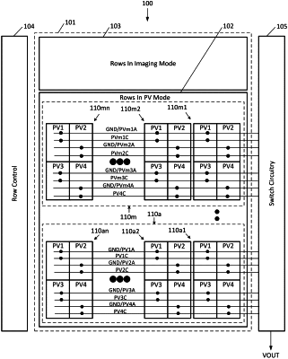
mode selection circuitry configured to control which groups of pixels of the pixel array operate in an imaging mode and which other groups of pixels of the pixel array operate in an energy harvesting mode; and
switch circuitry configured to selectively connect photodiodes of different groups of pixels in rows operating in the energy harvesting mode into one of: forward biased series configurations between a voltage output line and a ground line, or forward biased parallel configurations between the voltage output line and the ground line;
wherein the switch circuitry connects photodiodes of a given group of pixels into the forward biased series configuration by directly electrically connecting a cathode of at least one photodiode of the given group of pixels to the ground line;
wherein the mode selection circuitry comprises, for each first pixel of a given group of pixels, an imaging selection transistor coupling an anode of the photodiode of that pixel to ground when in the imaging mode and an energy harvesting selection transistor coupling a cathode of the photodiode of that pixel to ground when in the energy harvesting mode; and
wherein the mode selection circuitry comprises, for each pixel of the given group of pixels other than the first pixel of the given group of pixels, an imaging selection transistor coupling an anode of the photodiode of that pixel to ground when in the imaging mode and an energy harvesting selection transistor coupling a cathode of the photodiode of that pixel to the switch circuitry for that pixel when in the energy harvesting mode; and
wherein the switch circuitry comprises, for each pixel of the given group of pixels except a last pixel of the given group of pixels:
a transmission gate selectively coupling the anode of the photodiode of that pixel to the energy harvesting selection transistor of a next pixel of the given group of pixels; and
a selection transistor selectively coupling the energy harvesting selection transistor of the next pixel of the given group of pixels to ground when the transmission gate is not coupling the anode of the photodiode of that pixel to the energy harvesting selection transistor of the next pixel of the given group of pixels.
|