| CPC H01L 27/1248 (2013.01) [H01L 21/02164 (2013.01); H01L 21/02282 (2013.01); H01L 27/1259 (2013.01); H01L 27/156 (2013.01); H10K 50/844 (2023.02); H10K 59/124 (2023.02); H10K 71/00 (2023.02); H10K 59/1201 (2023.02)] | 3 Claims |
|
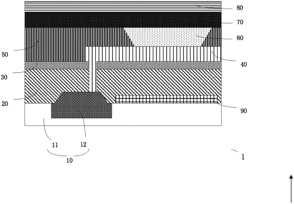
1. A production method for a display device, wherein the production method comprises
providing a base substrate;
covering the base substrate with an organic planarization layer;
covering a side of the organic planarization layer away from the base substrate with a transparent electric insulating heat conductive protective layer against deformation due to sputtering; and
forming a light-emitting element at a side of the transparent electric insulating heat conductive protective layer against deformation due to sputtering away from the base substrate;
wherein an orthographic projection of the light-emitting element on the base substrate and an orthographic projection of the transparent electric insulating heat conductive protective layer against deformation due to sputtering on the base substrate at least partially overlap,
wherein said covering a side of the organic planarization layer away from the base substrate with a transparent electric insulating heat conductive protective layer against deformation due to sputtering comprises:
producing a silica sol;
applying the silica sol on a side of the organic planarization layer away from the base substrate;
heating and curing the silica sol, so as to obtain a nano silica thin film layer,
wherein said producing a silica sol comprises
mixing ethyl orthosilicate with a solvent, then adding a basic catalyst and performing stirring;
adding N, N-dimethyl formamide, and obtaining the silica sol after stirring,
wherein the basic catalyst comprises a mixture of ammonia and water with a molar ratio of 0.001-0.002,
wherein a volume fraction of the N, N-dimethyl formamide in the silica sol is 25%-35%.
|