| CPC H01L 27/124 (2013.01) [H01L 27/1255 (2013.01); H01L 27/156 (2013.01); H10K 59/1213 (2023.02)] | 18 Claims |
|
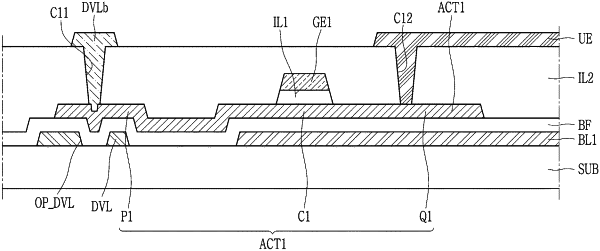
1. A display device comprising:
a metal layer disposed on a substrate;
a transistor disposed on the metal layer; and
a light emitting element electrically connected to the transistor, wherein
the transistor includes a semiconductor layer at least partially overlapping the metal layer,
the semiconductor layer includes a first region, a second region, and a channel region disposed between the first region and the second region,
the metal layer overlaps the second region and the channel region and is spaced apart from the first region in a plan view; and
a driving voltage line that overlaps a portion of the semiconductor layer, wherein
the driving voltage line and the metal layer are spaced apart from each other.
|