| CPC H01L 27/124 (2013.01) | 13 Claims |
|
1. An array substrate, comprising:
a substrate;
a plurality of active switches formed above the substrate; and
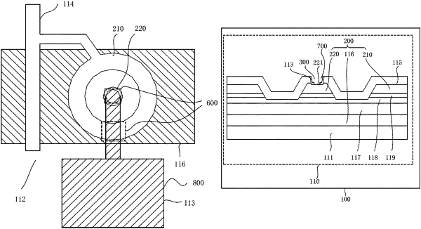
a transparent conductive layer formed above the active switches and connected to each of the active switches, wherein
each of the active switches comprises a metal layer; and
a hollow structure disposed through the transparent conductive layer, and located in an overlapping region between the transparent conductive layer and the metal layer;
wherein the metal layer includes a drain metal layer, and the transparent conductive layer includes a connection section connected to the drain metal layer; and the hollow structure includes a hollowed structure located in an overlapping region between the connection section and the drain metal layer;
wherein the drain metal layer and the hollowed structure are circular;
wherein the drain metal layer and the hollowed structure are concentric circles.
|