| CPC H01L 27/124 (2013.01) [H01L 27/1259 (2013.01); G09G 3/006 (2013.01); G09G 2330/12 (2013.01)] | 10 Claims |
|
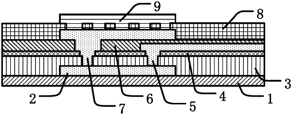
1. An array substrate, comprising a terminal region,
wherein a testing electric circuit wiring is disposed in the terminal region, and the terminal region comprises a pixel electrode,
wherein the testing electric circuit wiring comprises:
a first metal layer configured to act as a light shielding layer and a signal transmitting line for a testing electric current of the testing electric circuit wiring;
a second metal layer configured to act as a gate electrode wiring, to transmit the testing electric current to gate electrodes; and
a third metal layer configured to act as a testing electric circuit, wherein the third metal layer is electrically connected to the pixel electrode, and the testing electric current is capable of transmitting between the third metal layer and the pixel electrode;
wherein the second metal layer is connected to the first metal layer, and
the third metal layer is connected to the first metal layer.
|