| CPC H01L 27/1218 (2013.01) [H01L 25/167 (2013.01); H01L 27/124 (2013.01); H01L 27/1262 (2013.01)] | 19 Claims |
|
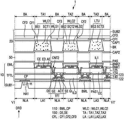
1. A display device comprising:
a first substrate comprising a first set of holes, wherein each of the first set of holes extends through the first substrate;
a first set of light emitting elements overlapping the first substrate;
a second set of light emitting elements overlapping the first substrate,
a first set of light blocking members;
a second set of light blocking members;
a first set of transistors, wherein each of the first set of transistors respectively overlaps each of the first set of light blocking members and respectively corresponds to each of the first set of light emitting elements; and
a second set of transistors, wherein each of the second set of transistors respectively overlaps each of the second set of light blocking members and respectively corresponds to each of the second set of light emitting elements, and wherein the each of the first set of holes is positioned between the first set of light blocking members and the second set of light blocking members in the plan view of the display device,
wherein the each of the first set of holes is positioned between the first set of light emitting elements and the second set of light emitting elements in a plan view of the display device.
|