| CPC H01L 27/092 (2013.01) [H01L 21/02057 (2013.01); H01L 21/28525 (2013.01); H01L 21/302 (2013.01); H01L 21/30608 (2013.01); H01L 21/3065 (2013.01); H01L 21/31138 (2013.01); H01L 21/47573 (2013.01); H01L 21/76801 (2013.01); H01L 21/823418 (2013.01); H01L 21/823437 (2013.01); H01L 21/823814 (2013.01); H01L 21/823821 (2013.01); H01L 23/485 (2013.01); H01L 27/0924 (2013.01); H01L 29/7848 (2013.01); H01L 29/165 (2013.01); H01L 29/41791 (2013.01); H01L 29/665 (2013.01)] | 20 Claims |
|
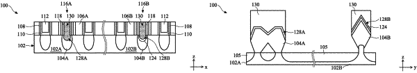
1. A semiconductor device, comprising:
an n-type transistor region including:
a first gate stack;
a first gate spacer over sidewalls of the first gate stack;
an n-type epitaxial feature in a source/drain (S/D) region of the n-type transistor region; and
a first metal silicide layer over the n-type epitaxial feature; and
a p-type transistor region including:
a second gate stack;
a second gate spacer over sidewalls of the second gate stack;
a p-type epitaxial feature in an S/D region of the p-type transistor region;
a dopant-containing implant layer over the p-type epitaxial feature, wherein the dopant-containing implant layer includes a metallic dopant; and
a second metal silicide layer over the dopant-containing implant layer,
wherein a top surface of the n-type epitaxial feature has a first concave profile, a top surface of the p-type epitaxial feature has a second concave profile, and a lowest point of the first concave profile is below a lowest point of the second concave profile.
|