| CPC H01L 27/067 (2013.01) [H01L 27/0262 (2013.01); H01L 29/6609 (2013.01); H01L 29/861 (2013.01); H01L 29/66371 (2013.01); H01L 29/732 (2013.01); H01L 29/7404 (2013.01)] | 6 Claims |
|
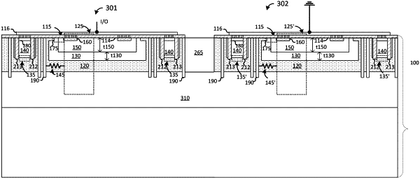
1. A method of forming a semiconductor device, the method comprising:
forming a first vertical protection device comprising a thyristor in a substrate;
forming a first lateral trigger element for triggering the first vertical protection device in the substrate; and
forming an electrical path in the substrate to electrically couple the first lateral trigger element with the first vertical protection device;
forming a second vertical protection device comprising a second thyristor in the substrate;
forming a second lateral trigger element for triggering the second vertical protection device in the substrate; and
forming a second electrical path in the substrate to electrically couple the second lateral trigger element with the second vertical protection device,
wherein the first and second vertical protection devices form a bidirectional transient voltage suppressor device,
wherein the first and second lateral trigger elements are each configured as bipolar transistors.
|