| CPC H01L 27/0248 (2013.01) [H01L 29/747 (2013.01); H01L 29/87 (2013.01)] | 20 Claims |
|
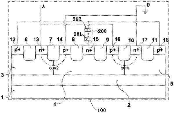
1. A diode-triggered bidirectional silicon controlled rectifier, comprising a silicon controlled rectifier (SCR) and a diode string, the silicon controlled rectifier having an anode and a cathode and comprising:
a P-type substrate;
a first P well formed in the P-type substrate, a first P-type doped region and a first N-type doped region being formed in the first P well;
a second P well formed in the P-type substrate, a third N-type doped region and a fourth P-type doped region being formed in the second P well; and
an N well formed in the P-type substrate, a second P-type doped region, a second N-type doped region and a third P-type doped region being formed in the N well;
wherein the first N-type doped region and the third P-type doped region are electrically connected with the anode; the third N-type doped region and the second P-type doped region are electrically connected with the cathode; the second N-type doped region is electrically connected with a positive electrode of the diode string, and the first P-type doped region and the fourth P-type doped region are electrically connected with a negative electrode of the diode string.
|