| CPC H01L 25/18 (2013.01) [H01L 23/5386 (2013.01); H01L 24/08 (2013.01); H01L 25/0655 (2013.01); H01L 25/50 (2013.01); H01L 24/06 (2013.01); H01L 24/94 (2013.01); H01L 2224/06152 (2013.01); H01L 2224/08145 (2013.01); H01L 2924/10156 (2013.01); H01L 2924/14511 (2013.01)] | 12 Claims |
|
1. A solid state drive (SSD) wafer device, comprising:
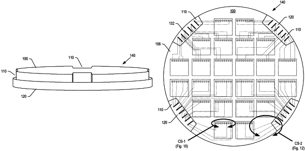
a first semiconductor wafer comprising first and second major surfaces, a plurality of memory dies, each memory die of the plurality of memory dies comprising a plurality of bond pads at the first major surface, and one or more cutouts; and
a second semiconductor wafer comprising third and fourth major surfaces, and a plurality of electrical interconnects, each electrical interconnect comprising a first terminal at the third major surface, at a first end of the electrical interconnect, and a second terminal at the third major surface, at a second end of the electrical interconnect opposite the first end, the second terminal of each of the electrical interconnects configured to transfer signals between the second semiconductor wafer and an external device;
wherein the first major surface of the first semiconductor wafer is coupled to the third major surface of the second semiconductor wafer, with the first terminal of each of the plurality of electrical interconnects bonded to a die bond pad of the plurality of die bond pads and the second terminal of each of the plurality of electrical interconnects positioned in the one or more cutouts.
|