| CPC H01L 25/105 (2013.01) [H01L 21/4857 (2013.01); H01L 21/486 (2013.01); H01L 21/565 (2013.01); H01L 23/3107 (2013.01); H01L 23/3128 (2013.01); H01L 23/49816 (2013.01); H01L 23/49822 (2013.01); H01L 23/49838 (2013.01); H01L 23/5226 (2013.01); H01L 23/5283 (2013.01); H01L 24/08 (2013.01); H01L 24/09 (2013.01); H01L 24/16 (2013.01); H01L 24/17 (2013.01); H01L 24/96 (2013.01); H01L 24/97 (2013.01); H01L 2224/0231 (2013.01); H01L 2224/02373 (2013.01); H01L 2224/02381 (2013.01); H01L 2224/08235 (2013.01); H01L 2224/16227 (2013.01); H01L 2224/96 (2013.01); H01L 2224/97 (2013.01); H01L 2225/1041 (2013.01); H01L 2225/1058 (2013.01); H01L 2924/182 (2013.01)] | 19 Claims |
|
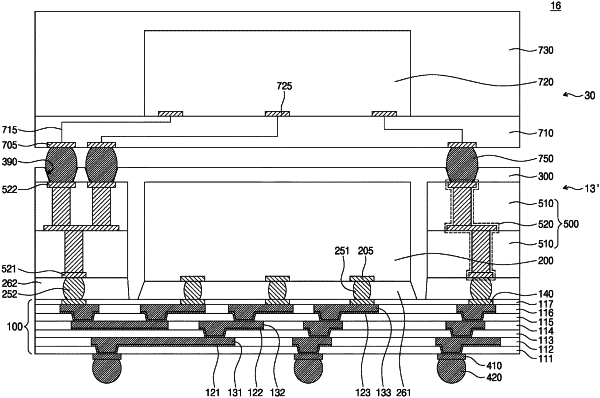
1. A semiconductor package, comprising:
a redistribution substrate;
a semiconductor chip on a top surface of the redistribution substrate; and
a solder ball on a bottom surface of the redistribution substrate,
wherein the redistribution substrate comprises:
a first insulating layer;
a redistribution pattern including a via portion in the first insulating layer and an interconnection portion connected to the via portion, the interconnection portion disposed on the first insulating layer;
a seed pattern covering a bottom surface and a side surface of the via portion and extending to a lower surface of the interconnection portion; and
a second insulating layer on the first insulating layer, the second insulating layer covering side surfaces of the interconnection portion,
wherein the seed pattern does not cover the side surfaces of the interconnection portion,
wherein the seed pattern is provided between the via portion and the solder ball, and
wherein a lowermost surface of the seed pattern is coplanar with a bottom surface of the first insulating layer.
|