| CPC H01L 25/0657 (2013.01) [H01L 21/76898 (2013.01); H01L 23/481 (2013.01); H01L 24/08 (2013.01); H01L 24/80 (2013.01); H01L 25/50 (2013.01); H01L 2224/08145 (2013.01); H01L 2224/80894 (2013.01); H01L 2225/06524 (2013.01); H01L 2225/06544 (2013.01); H01L 2225/06593 (2013.01)] | 20 Claims |
|
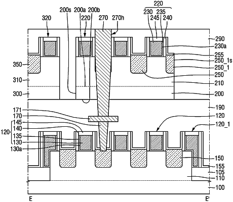
1. A method of fabricating a semiconductor device, the method comprising:
forming, in a first active region of a lower semiconductor substrate, a plurality of lower transistors, which comprise a plurality of lower gate structures and a plurality of lower source/drain regions;
forming, on the lower semiconductor substrate, a lower interlayer insulating film, covering the plurality of lower gate structures and the plurality of lower source/drain regions;
forming, in an upper semiconductor substrate, a plurality of upper transistors, which comprise a plurality of upper gate structures and a plurality of upper source/drain regions;
bonding the upper semiconductor substrate onto the lower interlayer insulating film;
after the bonding of the upper semiconductor substrate onto the lower interlayer insulating film, performing a first etching process to remove some of the plurality of upper gate structures and some of the plurality of upper source/drain regions;
after the bonding of the upper semiconductor substrate onto the lower interlayer insulating film, performing a second etching process to partially remove the upper semiconductor substrate; and
after the first etching process and the second etching process, forming a connection contact, connecting at least one of the plurality of lower transistors to at least one of the plurality of upper transistors.
|