| CPC H01L 25/0655 (2013.01) [H01L 23/3121 (2013.01); H01L 24/16 (2013.01); H01L 24/32 (2013.01); H01L 24/33 (2013.01); H01L 24/48 (2013.01); H01L 24/73 (2013.01); H01L 25/0652 (2013.01); H01L 2224/16225 (2013.01); H01L 2224/32145 (2013.01); H01L 2224/32225 (2013.01); H01L 2224/33181 (2013.01); H01L 2224/48225 (2013.01); H01L 2224/73204 (2013.01); H01L 2224/73215 (2013.01); H01L 2224/73265 (2013.01)] | 20 Claims |
|
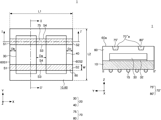
1. A semiconductor package, comprising:
a substrate;
a first semiconductor chip structure on the substrate and a second semiconductor chip structure on the substrate, the first semiconductor chip structure and the second semiconductor chip structure being spaced apart from each other in a first horizontal direction that is parallel to an upper surface of the substrate;
a mold layer on the substrate, the mold layer covering both the first semiconductor chip structure and the second semiconductor chip structure;
a supporting structure on the mold layer, the supporting structure distal from the upper surface of the substrate than both the first semiconductor chip structure and the second semiconductor chip structure in a vertical direction that is perpendicular to the upper surface of the substrate, the supporting structure being in direct contact with the mold layer;
a lower semiconductor package; and
conductive bumps electrically connecting the lower semiconductor package and the substrate,
wherein the lower semiconductor package includes a lower substrate, one or more lower semiconductor chips on the lower substrate, and connection conductive patterns on the lower substrate and electrically connected to the conductive bumps,
wherein the supporting structure includes a first supporting structure and a second supporting structure, the first supporting structure and the second supporting structure being spaced apart from each other in a second horizontal direction that is parallel to the upper surface of the substrate, and further is perpendicular to the first horizontal direction,
wherein each of the first supporting structure and the second supporting structure has a first bar shape or a first linear shape extending in the first horizontal direction, and
wherein at least one of the first supporting structure or the second supporting structure overlaps the first and second semiconductor chip structures in the vertical direction.
|