| CPC H01L 25/0652 (2013.01) [H01L 23/3107 (2013.01); H01L 23/367 (2013.01); H01L 23/49811 (2013.01); H01L 23/49822 (2013.01); H01L 23/66 (2013.01); H01L 24/16 (2013.01); H01L 2223/6677 (2013.01); H01L 2224/16227 (2013.01)] | 18 Claims |
|
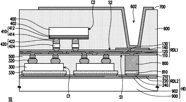
1. An integrated antenna package structure, comprising:
a first redistribution structure comprising a plurality of first conductive layers and a plurality of first insulating layers overlapping the plurality of first conductive layers;
a first chip located on a first side of the first redistribution structure and electrically connected to the first redistribution structure;
a heat dissipation structure thermally connected to the first chip, wherein the first chip is located between the heat dissipation structure and the first redistribution structure;
a second chip located on a second side of the first redistribution structure opposite to the first side and electrically connected to the first redistribution structure, wherein one of the plurality of first conductive layers is located between the first chip and the second chip; and
an antenna structure electrically connected to the first redistribution structure, wherein the antenna structure extends continuously to contact a top surface of the one of the plurality of first conductive layers.
|