| CPC H01L 25/0652 (2013.01) [H01L 21/4853 (2013.01); H01L 21/56 (2013.01); H01L 23/3121 (2013.01); H01L 23/49827 (2013.01); H01L 23/49833 (2013.01); H01L 23/552 (2013.01); H01L 25/16 (2013.01); H01L 25/50 (2013.01)] | 13 Claims |
|
1. A method for fabricating an electronic package, comprising:
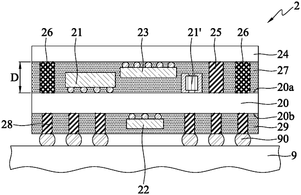
providing a first carrying structure having a first surface and a second surface opposing the first surface, with at least one first electronic component disposed on the first surface and electrically connected to the first carrying structure, and a plurality of conductors disposed on the second surface and electrically connected to the first carrying structure;
stacking on the first surface of the first carrying structure via at least one conductive element in a vertical direction a second carrying structure provided with a functional electronic component, wherein a lateral side surface of the functional electronic component faces and partially overlaps a lateral side surface of the first electronic component in a horizontal direction perpendicular to the vertical direction, and a top side surface of the functional electronic component does not face and overlap a top side surface of the first electronic component in the vertical direction; and
forming a packaging layer between the first carrying structure and the second carrying structure, allowing the packaging layer to pack the first electronic component, the functional electronic component and the conductive element.
|