| CPC H01L 24/83 (2013.01) [H01L 24/27 (2013.01); H01L 24/32 (2013.01); H01L 25/0753 (2013.01); H01L 33/62 (2013.01); H01L 2224/2744 (2013.01); H01L 2224/32227 (2013.01); H01L 2224/83005 (2013.01); H01L 2224/83143 (2013.01); H01L 2224/83203 (2013.01); H01L 2224/83851 (2013.01); H01L 2224/83862 (2013.01); H01L 2224/83868 (2013.01); H01L 2224/83871 (2013.01); H01L 2224/83874 (2013.01); H01L 2224/83986 (2013.01)] | 4 Claims |
|
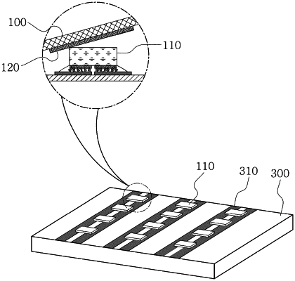
1. An electronic device, comprising:
a substance;
a pair of electrodes extending in one direction, the pair of electrodes on at least one surface of the substance;
a plurality of electronic elements, each of the plurality of electronic elements arranged perpendicularly across the pair of electrodes to form an array aligned with each other; and
a plurality of cured polymers between the plurality of electronic elements and the pair of electrodes and spaced apart from each other by forming an island structure;
wherein each of the plurality of electronic elements has at least one contact pad on at least one surface facing at least one of the pair of electrodes for electrical connection,
wherein the plurality of cured polymers include a plurality of ferromagnetic particles arranged in one direction, and the pair of electrodes and a plurality of contact pads of the plurality of electronic elements are electrically connected through the plurality of ferromagnetic particles,
wherein the at least one of the pair of electrodes include a structure formed extending in at least one direction,
wherein the at least one direction in which the at least one of the pair of electrodes extends and the one direction in which the plurality of ferromagnetic particles are arranged are perpendicular to each other,
at least some of the plurality of cured polymers are formed in a form in which a planar area is wider than a planar area of the electronic device and surrounds the electronic device when viewed from above,
wherein each of the plurality of electronic elements is a micro light emitting diode (LED).
|