| CPC H01L 24/32 (2013.01) [H01L 24/05 (2013.01); H01L 24/13 (2013.01); H01L 24/16 (2013.01); H01L 24/27 (2013.01); H01L 24/29 (2013.01); H01L 24/83 (2013.01); H01L 25/105 (2013.01); H01L 24/03 (2013.01); H01L 24/11 (2013.01); H01L 24/20 (2013.01); H01L 24/48 (2013.01); H01L 24/81 (2013.01); H01L 2224/0345 (2013.01); H01L 2224/03462 (2013.01); H01L 2224/03464 (2013.01); H01L 2224/0347 (2013.01); H01L 2224/03912 (2013.01); H01L 2224/0401 (2013.01); H01L 2224/04026 (2013.01); H01L 2224/04105 (2013.01); H01L 2224/05017 (2013.01); H01L 2224/05024 (2013.01); H01L 2224/05147 (2013.01); H01L 2224/05166 (2013.01); H01L 2224/05558 (2013.01); H01L 2224/05572 (2013.01); H01L 2224/05624 (2013.01); H01L 2224/05647 (2013.01); H01L 2224/05666 (2013.01); H01L 2224/05684 (2013.01); H01L 2224/1144 (2013.01); H01L 2224/1145 (2013.01); H01L 2224/11462 (2013.01); H01L 2224/12105 (2013.01); H01L 2224/13019 (2013.01); H01L 2224/131 (2013.01); H01L 2224/13124 (2013.01); H01L 2224/13147 (2013.01); H01L 2224/13166 (2013.01); H01L 2224/13184 (2013.01); H01L 2224/16145 (2013.01); H01L 2224/16227 (2013.01); H01L 2224/27462 (2013.01); H01L 2224/29026 (2013.01); H01L 2224/32145 (2013.01); H01L 2224/32148 (2013.01); H01L 2224/32225 (2013.01); H01L 2224/48091 (2013.01); H01L 2224/48227 (2013.01); H01L 2224/73265 (2013.01); H01L 2224/73267 (2013.01); H01L 2224/81121 (2013.01); H01L 2224/81125 (2013.01); H01L 2224/81193 (2013.01); H01L 2224/81801 (2013.01); H01L 2224/81815 (2013.01); H01L 2224/81895 (2013.01); H01L 2224/8191 (2013.01); H01L 2225/0651 (2013.01); H01L 2225/06568 (2013.01); H01L 2225/1035 (2013.01); H01L 2225/1058 (2013.01); H01L 2924/1203 (2013.01); H01L 2924/1205 (2013.01); H01L 2924/1206 (2013.01); H01L 2924/1207 (2013.01); H01L 2924/15311 (2013.01); H01L 2924/181 (2013.01)] | 20 Claims |
|
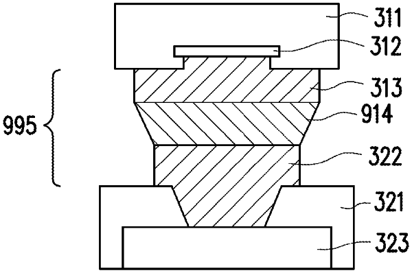
1. A device comprising:
a first semiconductor device comprising a first contact pad having a first surface contacting a metal feature, the first contact pad having a second surface opposite the first surface, the second surface being planar, wherein a ratio of a first width of the first surface to a second width of the second surface is 2:5;
a solder layer bonded to the first contact pad; and
a second semiconductor device comprising a second contact pad, the second contact pad having a third surface bonded to the solder layer, the second contact pad having a fourth surface opposite the third surface, the third surface being planar, wherein a ratio of a third width of the third surface to a fourth width of the fourth surface is 5:2, wherein the solder layer has tapered sidewalls continuously diminishing from the second width at a fifth surface adjoining the first contact pad to the third width at a sixth surface adjoining the second contact pad.
|