| CPC H01L 24/32 (2013.01) [H01L 23/49513 (2013.01); H01L 23/49558 (2013.01); H01L 23/49575 (2013.01); H01L 23/49582 (2013.01); H01L 23/49586 (2013.01); H01L 23/5329 (2013.01); H01L 24/27 (2013.01); H01L 24/29 (2013.01); H01L 24/83 (2013.01); H01L 23/053 (2013.01); H01L 23/49503 (2013.01)] | 18 Claims |
|
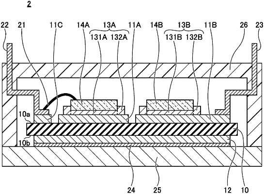
1. A semiconductor device, comprising:
a chip mounting member; and
a semiconductor chip bonded to the chip mounting member through a metal sintered material,
wherein the metal sintered material includes a first portion exactly overlapping the semiconductor chip in a plan view, and includes a second portion surrounding the first portion in the plan view, the first portion and the second portion being arranged next to each other without a gap therebetween,
wherein a porosity ratio of the first portion is lower than a porosity ratio of the second portion, and
wherein a thickness of the first portion is less than a thickness of any part of the second portion.
|