| CPC H01L 24/32 (2013.01) [H01L 21/52 (2013.01); H01L 23/48 (2013.01); H01L 24/29 (2013.01); H01L 24/30 (2013.01); H01L 24/33 (2013.01); H01L 24/83 (2013.01); H01L 2224/26155 (2013.01); H01L 2224/29155 (2013.01); H01L 2224/30181 (2013.01); H01L 2224/32245 (2013.01); H01L 2224/33181 (2013.01); H01L 2224/83007 (2013.01); H01L 2224/83065 (2013.01); H01L 2224/83815 (2013.01); H01L 2924/014 (2013.01); H01L 2924/10272 (2013.01); H01L 2924/351 (2013.01)] | 19 Claims |
|
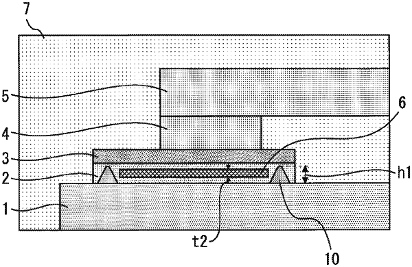
1. A semiconductor device comprising:
an electrode substrate;
a semiconductor chip bonded to an upper surface of the electrode substrate via a first solder;
a lead frame bonded to an upper surface of the semiconductor chip via a second solder;
an intermediate plate provided in the first solder between the electrode substrate and the semiconductor chip; and
a plurality of bumps provided between the electrode substrate and the semiconductor chip, the plurality of bumps being comprised of wire,
wherein a yield strength of the intermediate plate is higher than yield strengths of the electrode substrate and the first solder within the whole operating temperature range of the semiconductor device,
an outermost periphery of the intermediate plate is positioned inward of an outer periphery of the semiconductor chip and the first solder in planar view,
the intermediate plate is positioned inward of the plurality of bumps in planar view, and
the uppermost height of the bumps is less than a total thickness of the first solder, such that the bump does not contact the semiconductor chip.
|