| CPC H01L 24/13 (2013.01) [H01L 24/03 (2013.01); H01L 24/05 (2013.01); H01L 24/11 (2013.01); H01L 2224/02371 (2013.01); H01L 2224/0401 (2013.01); H01L 2224/05551 (2013.01)] | 20 Claims |
|
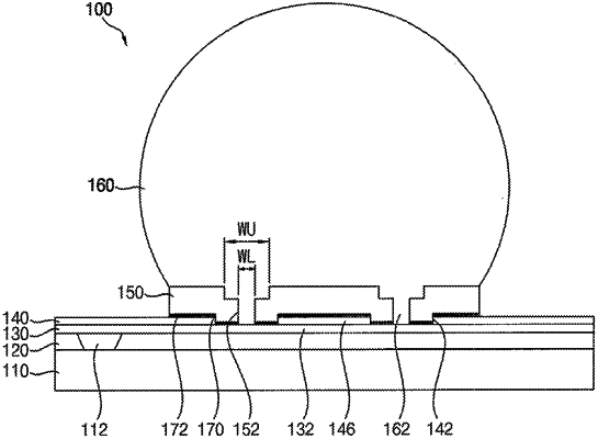
1. A semiconductor package, comprising:
a semiconductor chip including a pad;
a first insulation pattern on an upper surface of the semiconductor chip and exposing the pad;
a redistribution layer (RDL) on an upper surface of the first insulation pattern and electrically connected to the pad;
a second insulation pattern on the upper surface of the first insulation pattern, the second insulation pattern including at least one opening that exposes a ball land of the RDL and at least one patterned portion located in the opening;
an under bump metal (UBM) on upper surfaces of the second insulation pattern and the patterned portion and filling the opening, the UBM including a first hole that exposes an edge portion of an upper surface of the ball land and at least one branch that crosses the first hole in a radial direction of the UBM; and
a conductive ball on an upper surface of the UBM, the conductive ball including a first locking portion in the first hole,
wherein the first hole has an area of about 10% to about 50% of an area of the upper surface of the UBM.
|