| CPC H01L 24/08 (2013.01) [G11C 16/08 (2013.01); G11C 16/10 (2013.01); H01L 24/80 (2013.01); H01L 25/0657 (2013.01); H01L 25/18 (2013.01); H01L 25/50 (2013.01); H10B 41/27 (2023.02); H10B 41/41 (2023.02); H10B 43/27 (2023.02); H10B 43/40 (2023.02); H01L 2224/08135 (2013.01); H01L 2224/80895 (2013.01); H01L 2224/80896 (2013.01); H01L 2924/1431 (2013.01); H01L 2924/14511 (2013.01)] | 10 Claims |
|
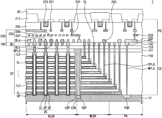
1. A semiconductor device, comprising a cell structure stacked on a peripheral circuit structure, wherein:
the cell structure includes:
a plurality of gate electrode layers stacked on a first substrate;
a plurality of channel regions vertically penetrating the gate electrode layers;
a first interlayer dielectric layer on the first substrate and covering the gate electrode layers and the channel regions; and
a plurality of first metal pads exposed at the first interlayer dielectric layer and connected to the gate electrode layers and the channel regions,
the peripheral circuit structure includes:
at least one transistor on a second substrate;
a second interlayer dielectric layer on the second substrate and covering the transistor; and
a plurality of second metal pads exposed at the second interlayer dielectric layer and connected to the transistor,
the plurality of first metal pads include at least one first sub-pad and at least one second sub-pad that are adjacent to each other,
the plurality of second metal pads include at least one third sub-pad and at least one fourth sub-pad that are adjacent to each other,
the at least one first sub-pad and the at least one third sub-pad are coupled to each other, and a width of the at least one first sub-pad is greater than a width of the at least one third sub-pad,
the at least one second sub-pad and the at least one fourth sub-pad are coupled to each other, and a width of the at least one fourth sub-pad is greater than a width of the at least one second sub-pad,
a distance between a lateral surface of the at least one first sub-pad and a lateral surface of the at least one second sub-pad adjacent to the at least one first sub-pad is substantially the same as a distance between a lateral surface of the at least one third sub-pad and a lateral surface of the at least one fourth sub-pad adjacent to the at least one third sub-pad, and
the width of the at least one first sub-pad is substantially the same as the width of the at least one fourth sub-pad, and the width of the at least one second sub-pad is substantially the same as the width of the at least one third sub-pad.
|