| CPC H01L 24/05 (2013.01) [H01L 24/03 (2013.01); H01L 2224/05026 (2013.01); H01L 2224/05082 (2013.01); H01L 2924/351 (2013.01)] | 16 Claims |
|
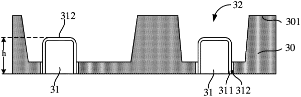
1. A method for forming a semiconductor structure, comprising:
providing a wafer having a front surface and a back surface opposite to the front surface, wherein at least one conductive plug provided in the wafer extends from the front surface towards the back surface;
patterning the back surface of the wafer to form at least one groove extending from the back surface towards the front surface, and exposing at least a portion of a surface of the at least one conductive plug;
forming a dielectric layer at a bottom and a side wall of the at least one groove; and
forming, on the dielectric layer, at least one conductive layer filling the at least one groove and extending from the back surface towards the front surface, wherein the at least one conductive layer is electrically connected to the at least one conductive plug.
|