| CPC H01L 24/03 (2013.01) [H01L 24/05 (2013.01); H01L 24/06 (2013.01); H01L 24/08 (2013.01); H01L 24/32 (2013.01); H01L 24/80 (2013.01); H01L 24/83 (2013.01); H01L 24/92 (2013.01); H01L 27/14607 (2013.01); H01L 27/14634 (2013.01); H01L 27/14636 (2013.01); H01L 27/14685 (2013.01); H01L 27/1469 (2013.01); H01L 2224/03019 (2013.01); H01L 2224/0346 (2013.01); H01L 2224/03845 (2013.01); H01L 2224/05567 (2013.01); H01L 2224/05571 (2013.01); H01L 2224/0603 (2013.01); H01L 2224/06135 (2013.01); H01L 2224/06136 (2013.01); H01L 2224/06177 (2013.01); H01L 2224/06517 (2013.01); H01L 2224/08146 (2013.01); H01L 2224/09517 (2013.01); H01L 2224/32145 (2013.01); H01L 2224/80075 (2013.01); H01L 2224/80895 (2013.01); H01L 2224/80896 (2013.01); H01L 2224/80948 (2013.01); H01L 2224/83075 (2013.01); H01L 2224/83948 (2013.01); H01L 2224/9211 (2013.01)] | 20 Claims |
|
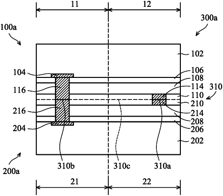
1. A semiconductor structure, comprising:
a first semiconductor device, wherein the first semiconductor device comprises:
a first oxide layer formed below the a first substrate;
a first bonding layer formed below the first oxide layer;
a first bonding via formed through the first bonding layer and the first oxide layer; and
a first dummy pad formed through the first bonding layer and adjacent to the first bonding via, wherein a first height of the first dummy pad is smaller than a second height of the first bonding via;
a second semiconductor device, wherein the second semiconductor device comprises:
a second oxide layer formed over a second substrate;
a second bonding layer formed over the second oxide layer; and
a second bonding via formed through the second bonding layer and the second oxide layer; and
a bonding structure between the first substrate and the second substrate, wherein the bonding structure comprises the first bonding via bonded to the second bonding via.
|