| CPC H01L 23/645 (2013.01) [H01L 23/49822 (2013.01); H01L 23/49838 (2013.01); H01L 23/49866 (2013.01)] | 12 Claims |
|
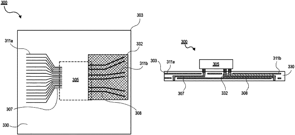
1. A package substrate, comprising:
a first conductive layer in a first magnetic layer;
a second magnetic layer over the first magnetic layer, wherein the first and second magnetic layers include a plurality of magnetic materials;
a second conductive layer in the second magnetic layer, wherein the second conductive layer includes a plurality of first traces, and wherein the plurality of first traces are fully surrounded by the first and second magnetic layers, wherein the second conductive layer further includes a plurality of second traces, wherein the plurality of first traces are a plurality of single-ended routing traces, wherein the plurality of second traces are a plurality of differential routing traces, wherein the plurality of single-ended routing traces have a width and a line spacing that is lower than a width and a line spacing of the plurality of differential routing traces, and wherein the plurality of single-ended routing traces and the plurality of differential routing traces are fully surrounded by the plurality of magnetic materials; and
a third conductive layer over the second magnetic layer, wherein the plurality of magnetic materials include manganese (Mn) ferrite materials, zinc (Zn) and Mn (Zn/Mn) ferrite materials, or nickel (Ni) and Zn (Ni/Zn) ferrite materials.
|