| CPC H01L 23/552 (2013.01) [H01L 21/4853 (2013.01); H01L 21/4889 (2013.01); H01L 21/565 (2013.01); H01L 23/3121 (2013.01); H01L 23/49 (2013.01); H01L 23/49838 (2013.01); H01L 24/16 (2013.01); H01L 2224/16227 (2013.01); H01L 2924/3025 (2013.01)] | 28 Claims |
|
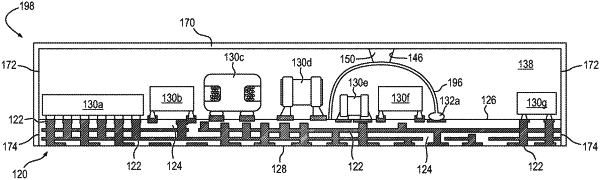
1. A method of making a semiconductor device, comprising:
providing a substrate;
disposing a bond wire on the substrate;
disposing an electrical component over the substrate, wherein the bond wire loops over the electrical component with a distal end of the bond wire returning to contact the substrate;
depositing an encapsulant over the substrate and bond wire;
forming an opening in the encapsulant extending below a surface of the encapsulant to a mid-portion of the bond wire; and
disposing a conductive material in the opening to contact the mid-portion of the bond wire.
|