| CPC H01L 23/552 (2013.01) [H01L 21/568 (2013.01); H01L 23/3128 (2013.01); H01L 23/5389 (2013.01)] | 5 Claims |
|
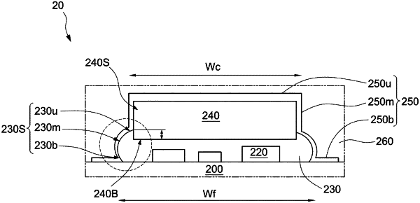
1. A semiconductor package, comprising:
a substrate having a first face;
at least one first electronic component mounted adjacent to a first region of the first face;
a plurality of second electronic components mounted adjacent to a second region of the first face;
an encapsulant disposed over the first and the second electronic components, wherein the encapsulant covers directly over the at least one first electronic component, and wherein the encapsulant covers the plurality of second electronic components through a layer of conductive material;
an insulating material disposed over and between the plurality of second electronic components; and
a cap member over the plurality of second electronic components and in contact with the insulating material,
wherein the insulating material defines a lateral surface covered by the layer of conductive material,
wherein an upper border of the insulating material is higher than a bottom surface of the cap member.
|