| CPC H01L 23/552 (2013.01) [H01L 23/3121 (2013.01); H01L 23/49811 (2013.01)] | 17 Claims |
|
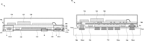
1. A semiconductor package, comprising:
a substrate having a first face and an opposing second face, wherein the first face is mounted with a first semiconductor component and a plurality of connectors; and
a first shielding member covering the first semiconductor component and a first group of the plurality of connectors, while exposing a second group of the plurality of connectors,
wherein the first semiconductor component is in physical contact with the first shielding member.
|