| CPC H01L 23/5384 (2013.01) [H01L 23/50 (2013.01); H01L 23/5286 (2013.01); H01L 23/5386 (2013.01); H01L 25/0657 (2013.01); H01L 23/481 (2013.01); H01L 23/49827 (2013.01); H01L 2224/08146 (2013.01); H01L 2225/06541 (2013.01)] | 38 Claims |
|
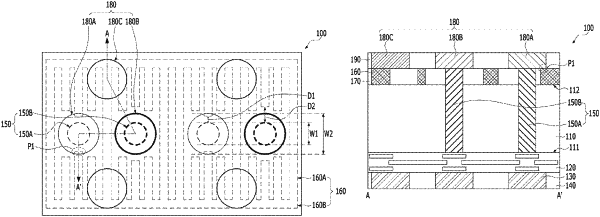
1. A semiconductor chip comprising:
a body portion with a front surface and a rear surface, the body portion being oriented in such a way that the rear surface is above the front surface;
first and second through electrodes penetrating the body portion with protrusions that protrude above the rear surface of the body portion;
a power pattern formed over the rear surface of the body portion and spaced apart from the protrusions;
an interlayer insulating layer filling spaces between the power pattern and the protrusions; and
first and second rear connection electrodes formed over the interlayer insulating layer and respectively connected to the first and second through electrodes,
wherein the first rear connection electrode is simultaneously connected to the first through electrode and a part of the power pattern that is adjacent to the first through electrode, and
wherein the second rear connection electrode is not connected to the power pattern.
|