| CPC H01L 23/5381 (2013.01) [H01L 23/5386 (2013.01); H01L 24/16 (2013.01); H01L 25/0652 (2013.01); H03K 19/17728 (2013.01); H03K 19/17744 (2013.01); H03K 19/1776 (2013.01); H03K 19/17764 (2013.01); H03K 19/17796 (2013.01); H01L 2224/16145 (2013.01); H01L 2224/16227 (2013.01); H01L 2224/16238 (2013.01); H01L 2924/14211 (2013.01); H01L 2924/1424 (2013.01); H01L 2924/1431 (2013.01); H01L 2924/14335 (2013.01); H01L 2924/30105 (2013.01); H01L 2924/30107 (2013.01); H01L 2924/37001 (2013.01)] | 17 Claims |
|
1. A multi-die FPGA implementing a built-in analog circuit using an active silicon connection layer, wherein the multi-die FPGA comprises a substrate, a silicon connection layer laminated on the substrate and a plurality of FPGA dies laminated on the silicon connection layer, the silicon connection layer covering all of the FPGA dies;
each FPGA die comprises a plurality of configurable functional modules, interconnection resource modules arranged around each of the configurable functional modules and connection point leads, the configurable functional modules within the FPGA die comprise at least a programmable logic block, a silicon stacked connection module and an input and output block, the silicon stacked connection module comprises a plurality of silicon stacked connection points, the programmable logic block within the FPGA die is connected to the silicon stack connection point and the input and output block respectively through the interconnection resource modules, the silicon stack connection points are connected to the corresponding connection point leads through top metal wires within a re-distribution layer; the connection point leads within each FPGA die are connected to the corresponding connection point leads in other FPGA dies through cross-die wires within the silicon connection layer, each FPGA die can be connected to any of the other FPGA dies through the cross-die wires within the silicon connection layer; the input and output block within the FPGA die is connected to the substrate through a silicon via within the silicon connection layer;
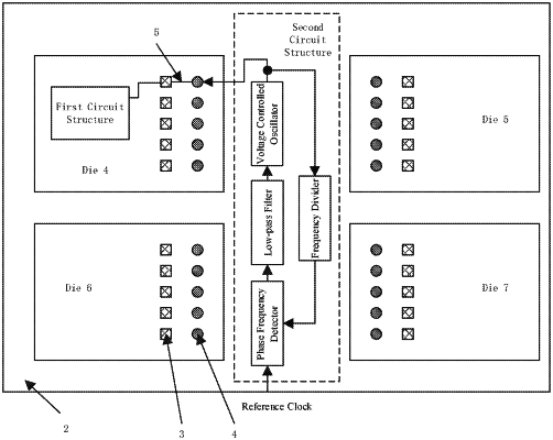
a first circuit structure is formed within the FPGA die, a port of the first circuit structure is connected to the corresponding silicon stack connection point via the interconnection resource module and then connected to the corresponding connection point lead through the top metal wire within the re-distribution layer;
a second circuit structure is laid out within the silicon connection layer, the second circuit structure comprises a plurality of analog circuit elements, the connection point leads within the FPGA die connected to the port of the first circuit structure is connected to a port of the second circuit structure through silicon connection layer wires within the silicon connection layer, the first circuit structure and the second circuit structure are connected to form a built-in analog circuit within the multi-die FPGA, the input and output block within the silicon connection layer is also connected to the substrate.
|