| CPC H01L 23/535 (2013.01) [H01L 21/76805 (2013.01); H01L 21/76895 (2013.01); H10B 41/27 (2023.02); H10B 43/27 (2023.02)] | 12 Claims |
|
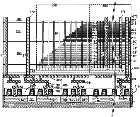
1. A semiconductor structure, comprising:
semiconductor devices located on a top surface of a substrate semiconductor layer;
lower-level metal interconnect structures embedded in lower-level dielectric material layers and electrically connected to the semiconductor devices and overlying the substrate semiconductor layer;
source-level material layers overlying the lower-level dielectric material layers and comprising an opening therethrough;
an alternating stack of insulating layers and electrically conductive layers overlying the source-level material layers;
memory stack structures vertically extending through the alternating stack and comprising a respective vertical semiconductor channel and a respective memory film;
a vertically alternating sequence of insulating plates and dielectric material plates laterally surrounded by the alternating stack;
an isolation trench fill structure interposed between the alternating stack and the vertically alternating sequence and comprising a trench fill material portion and a capping dielectric structure overlying the trench fill material portion; and
a first through-memory-level interconnection via structure vertically extending through each plate within the vertically alternating sequence and contacting a top surface of one of the lower-level metal interconnect structures;
wherein the isolation trench fill structure comprises a first straight sidewall contacting the alternating stack and a second straight sidewall contacting the vertically alternating sequence, wherein each of the first straight sidewall and the second straight sidewall vertically extends from a horizontal plane overlying a topmost surface of the alternating stack into an upper region of the source-level material layers.
|
|
3. A semiconductor structure, comprising:
semiconductor devices located on a top surface of a substrate semiconductor layer;
lower-level metal interconnect structures embedded in lower-level dielectric material layers and electrically connected to the semiconductor devices and overlying the substrate semiconductor layer;
source-level material layers overlying the lower-level dielectric material layers and comprising an opening therethrough;
an alternating stack of insulating layers and electrically conductive layers overlying the source-level material layers;
memory stack structures vertically extending through the alternating stack and comprising a respective vertical semiconductor channel and a respective memory film;
a vertically alternating sequence of insulating plates and dielectric material plates laterally surrounded by the alternating stack;
an isolation trench fill structure interposed between the alternating stack and the vertically alternating sequence and comprising a trench fill material portion and a capping dielectric structure overlying the trench fill material portion; and
a first through-memory-level interconnection via structure vertically extending through each plate within the vertically alternating sequence and contacting a top surface of one of the lower-level metal interconnect structures;
wherein the trench fill material portion comprises a semiconductor material.
|
|
5. A semiconductor structure, comprising:
semiconductor devices located on a top surface of a substrate semiconductor layer;
lower-level metal interconnect structures embedded in lower-level dielectric material layers and electrically connected to the semiconductor devices and overlying the substrate semiconductor layer;
source-level material layers overlying the lower-level dielectric material layers and comprising an opening therethrough;
an alternating stack of insulating layers and electrically conductive layers overlying the source-level material layers;
memory stack structures vertically extending through the alternating stack and comprising a respective vertical semiconductor channel and a respective memory film;
a vertically alternating sequence of insulating plates and dielectric material plates laterally surrounded by the alternating stack;
an isolation trench fill structure interposed between the alternating stack and the vertically alternating sequence and comprising a trench fill material portion and a capping dielectric structure overlying the trench fill material portion; and
a first through-memory-level interconnection via structure vertically extending through each plate within the vertically alternating sequence and contacting a top surface of one of the lower-level metal interconnect structures;
a backside trench vertically extending through the alternating stack;
a backside contact via structure located within the backside trench, contacting one of the source-level material layers, and comprising a same material as the first through-memory-level interconnection via structure; and
a backside insulating spacer laterally surrounding the backside contact via structure and contacting each layer within the alternating stack.
|
|
12. A semiconductor structure, comprising:
semiconductor devices located on a top surface of a substrate semiconductor layer;
lower-level metal interconnect structures embedded in lower-level dielectric material layers and electrically connected to the semiconductor devices and overlying the substrate semiconductor layer;
source-level material layers overlying the lower-level dielectric material layers and comprising an opening therethrough;
an alternating stack of insulating layers and electrically conductive layers overlying the source-level material layers;
memory stack structures vertically extending through the alternating stack and comprising a respective vertical semiconductor channel and a respective memory film;
a vertically alternating sequence of insulating plates and dielectric material plates laterally surrounded by the alternating stack;
an isolation trench fill structure interposed between the alternating stack and the vertically alternating sequence and comprising a trench fill material portion and a capping dielectric structure overlying the trench fill material portion; and
a first through-memory-level interconnection via structure vertically extending through each plate within the vertically alternating sequence and contacting a top surface of one of the lower-level metal interconnect structures;
wherein the capping dielectric structure comprises:
a planar top surface within a first horizontal plane overlying a topmost surface of the alternating stack; and
a bottom surface located below a second horizontal plane including the topmost surface of the alternating stack and contacting a top surface of the trench fill material portion.
|