| CPC H01L 23/5286 (2013.01) [H01L 23/36 (2013.01); H01L 23/481 (2013.01); H01L 23/5226 (2013.01); H01L 24/08 (2013.01); H01L 2224/08145 (2013.01)] | 20 Claims |
|
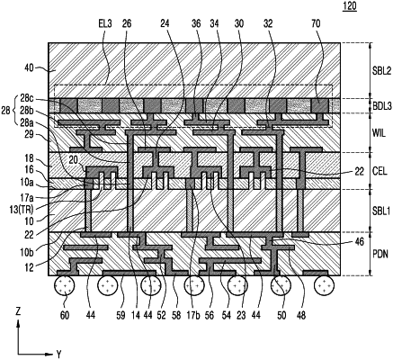
18. An integrated circuit semiconductor device comprising:
a substrate having a first surface and a second surface opposite the first surface;
a rail through via passing between the first surface and the second surface of the substrate;
a cell-level portion arranged on the first surface and comprising a buried rail connected to the rail through via, a local conductive interconnect, a cell via connected to the local conductive interconnect, and a transistor connected to the local conductive interconnect;
a signal wiring-level portion arranged on the cell-level portion and comprising a plurality of upper multi-layer interconnect layers connected to the local conductive interconnect via the cell via and upper vias connecting the upper multi-layer interconnect layers to each other;
a dummy substrate arranged on the signal wiring-level portion;
a bonding-level portion arranged between the signal wiring-level portion and the dummy substrate and bonding the signal wiring-level portion to the dummy substrate, and comprising a bonding pad connected to an upper via of the upper vias;
a power delivery network-level portion arranged under the second surface of the substrate and comprising a plurality of lower multi-layer interconnect layers connected to the rail through via and lower vias connecting the lower multi-layer interconnect layers to each other; and
an external connection terminal arranged under the power delivery network-level portion and connected to the lower multi-layer interconnect layers.
|