| CPC H01L 23/5283 (2013.01) [H01L 21/32133 (2013.01); H01L 21/32139 (2013.01); H01L 21/76802 (2013.01); H01L 21/76837 (2013.01); H01L 21/76877 (2013.01); H01L 21/76883 (2013.01); H01L 21/76885 (2013.01); H01L 21/76897 (2013.01); H01L 23/5226 (2013.01)] | 20 Claims |
|
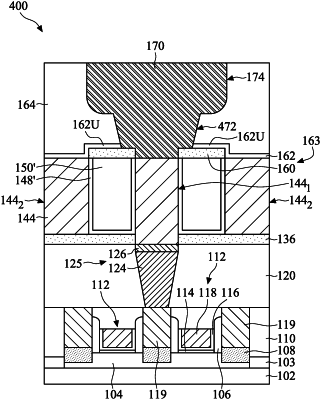
1. An interconnect structure, comprising:
a first via in a first dielectric layer;
a first metal line on and electrically connected to the first via;
a first etching stop layer over the first dielectric layer;
a second metal line over the first etching stop layer;
an encapsulating layer including a first vertical portion along a sidewall of the first metal line, a horizontal portion along an upper surface of the first etching stop layer, and a second vertical portion along a sidewall of the second metal line;
a second dielectric layer nested within the encapsulating layer;
a second etching stop layer over and in contact with a top surface of the first vertical portion and a top surface of the second vertical portion of the encapsulating layer and a top surface of the second dielectric layer; and
a third etching stop layer over and in contact with a top surface of the second metal line.
|
|
10. An interconnect structure, comprising:
a first metal line and a second metal line in a first dielectric layer;
a first etching stop layer over the first metal line, the second metal line and the first dielectric layer, wherein the first etching stop layer includes a first portion directly above the second metal line and a second portion directly above the first dielectric layer, and the second portion of the first etching stop layer is thicker than the first portion of the first etching stop layer, and a bottom surface of the second portion of the first etching stop layer is substantially level to a bottom surface of the first portion of the first etching stop layer;
a second dielectric layer over the first etching stop layer;
a first via extending through the second dielectric layer and the first etching stop layer and landing on the first metal line;
a second etching stop layer below the second metal line and the first dielectric layer and surrounding a lower portion of the first metal line; and
an encapsulating layer including a first portion extending between the first metal line and the first dielectric layer, a second portion extending between the second metal line and the first dielectric layer and a third portion extending between the second etching stop layer and the first dielectric layer, wherein the encapsulating layer and the first dielectric layer are made of different materials.
|
|
15. An interconnect structure, comprising:
a first interconnect layer comprising a first via through a first dielectric layer;
a second interconnect layer over the first interconnect layer, comprising:
a first self-aligned etching stop layer;
a second dielectric layer over the first self-aligned etching stop layer;
a first metal line through the second dielectric layer and the first self-aligned etching stop layer and landing on the first via; and
an encapsulating layer extending between the first self-aligned etching stop layer and the second dielectric layer and between the first metal line and the second dielectric layer,
wherein the first via includes a metal capping layer in direct contact with the first metal line, and a sidewall of the metal capping layer is aligned with a sidewall of the first metal line; and
a third interconnect layer over the second interconnect layer, comprising:
a second self-aligned etching stop layer along an upper surface of the second dielectric layer;
a conformal etching stop layer along an upper surface and a sidewall of the second self-aligned etching stop layer;
a third dielectric layer over the conformal etching stop layer; and
a second via through the third dielectric layer, the conformal etching stop layer and the second self-aligned etching stop layer and landing on the first metal line,
wherein the second self-aligned etching stop layer extends beyond an end of the conformal etching stop layer, and the second via further lands on a portion of the second self-aligned etching stop layer extending beyond the conformal etching stop layer.
|