| CPC H01L 23/5283 (2013.01) [H01L 21/76816 (2013.01); H01L 21/76877 (2013.01); H01L 23/528 (2013.01); H10B 43/10 (2023.02); H10B 43/27 (2023.02); H10B 43/40 (2023.02); H10B 43/50 (2023.02)] | 14 Claims |
|
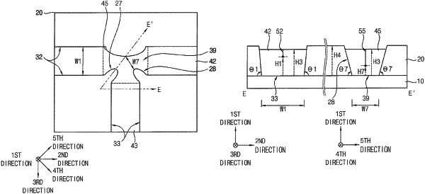
1. A wiring structure, comprising:
a first metal pattern on a substrate, the first metal pattern extending in a second direction that is parallel to an upper surface of the substrate and having a first width in a third direction that is parallel to the upper surface of the substrate and perpendicular to the second direction;
a second metal pattern extending in the third direction and having a second width in the second direction; and
a third metal pattern connected to the first and second metal patterns and located at an area where a central portion of the first metal pattern meets an end portion of the second metal pattern, the third metal pattern having a substantially rectangular shape including first and second sides facing each other in the third direction, the second side of the substantially rectangular shape being free from contact with the second metal pattern and concave, and a third width defined as a minimum distance between the first and second sides of the third metal pattern in the third direction being less than or equal to a smaller of the first and second widths,
wherein each metal pattern has a boundary surface at a central portion thereof, each boundary surface extending in a first direction perpendicular to the upper surface of the substrate, and
wherein a bottom of each of the boundary surfaces of the first and second metal patterns is farther from the substrate than a bottom of the boundary surface of the third metal pattern.
|
|
5. A wiring structure, comprising:
a first metal pattern on a substrate, the first metal pattern extending in a second direction that is parallel to an upper surface of the substrate and having a first width in a third direction that is parallel to the upper surface of the substrate and perpendicular to the second direction;
a second metal pattern extending in the third direction and having a second width in the second direction; and
a third metal pattern connected to the first and second metal patterns and located at an area where the first and second metal patterns cross or meet each other, wherein a minimum width between portions of the third metal pattern in a fourth direction parallel to the upper surface of the substrate and having an acute angle with respect to each of the second and third directions is equal to or less than the first width,
wherein an angle of a sidewall of the first metal pattern with respect to a first direction perpendicular to the upper surface of the substrate and an angle of a sidewall of the second metal pattern with respect to the first direction are both greater than an angle of a sidewall of the third metal pattern with respect to the first direction.
|
|
11. A wiring structure, comprising:
a first metal pattern on a substrate, the first metal pattern extending in a second direction that is parallel to an upper surface of the substrate and having a first width in a third direction that is parallel to the upper surface of the substrate and perpendicular to the second direction;
a second metal pattern extending in the third direction and having a second width in the second direction;
a third metal pattern connected to the first and second metal patterns and located at an area where the first and second metal patterns cross or meet each other; and
an insulating interlayer that covers sidewalls of the first to third metal patterns on the substrate,
wherein a minimum width between portions of the third metal pattern in a fourth direction parallel to the upper surface of the substrate and having an acute angle with respect to each of the second and third directions is equal to or less than the first width,
wherein an angle of a sidewall of the first metal pattern with respect to a first direction perpendicular to the upper surface of the substrate and an angle of a sidewall of the second metal pattern with respect to the first direction are both greater than an angle of a sidewall of the third metal pattern with respect to the first direction, and
wherein each of the first, second, and third metal patterns has a boundary surface at a central portion thereof.
|